GaN in PSUs
Advantages and Challenges of GaN in Power Supply Designs
Rapid semiconductor advancements over the past decade have delivered a range of very fast switching super junction MOSFETs. By adapting existing power supply designs and moving to new topologies, these devices deliver efficiency improvements, smaller form factors, and reductions in heat dissipation – all benefits that industrial, telecoms, and computing customers are keen to leverage.
But something new is vying for space on the printed circuit board – wide bandgap devices (WBG). These offer lower on-resistance and higher switching speeds than traditional silicon transistors, leading to more efficient and smaller power converters. On top of that, they also offer less parasitic capacitance, which is crucial for attaining higher switching speeds.
There is, however, a fly in the ointment – WBG devices are more expensive. This means they must deliver cost savings elsewhere, either in a reduced bill-of-materials, at system level, or through operating costs. Furthermore, the approach to driving their gates and dealing with the impact of higher switching frequencies must be mastered before deploying them in products that must operate reliably for a decade or more.
Features of WBG
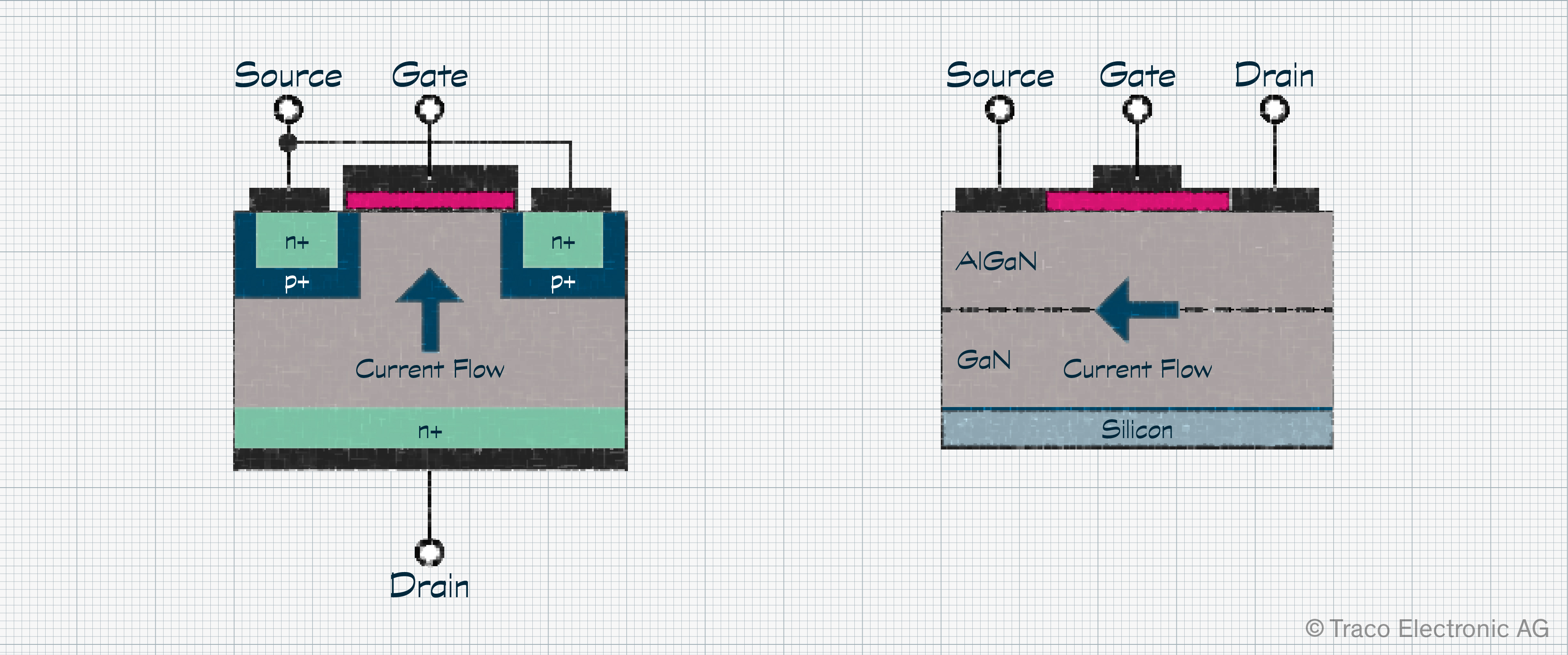
There are two competing WBG technologies. The first is Gallium Nitride, or GaN; the second is Silicon Carbide, or SiC (Figure 1). SiC devices are available with a VDS of around 650 V to 2,200 V. They’re well suited to applications with high reverse voltages, are robust, and the body diode offers a very short reverse recovery time. Switching speeds range from tens- to hundreds of kilohertz. However, gate control can be challenging, with negative voltages sometimes needed to avoid unwanted turn-on in some topologies.
GaN devices come in two types: D-mode, which are normally on, and E-mode, which are normally off. Thus, the optimal gate drive approach varies between suppliers. VDS ranges from 30 V to 900 V and, unlike MOSFETs, there is no body diode and associated reverse-recovery losses. Switching frequencies can reach several megahertz thanks to the much shorter switching time. Perhaps one of the greatest difficulties is in the gate drive circuitry, with the currents and frequencies involved making circuit robustness challenging. Some suppliers are already integrating gate drive circuitry to mitigate this, but this complicates second sourcing.
Overall, GaN and SiC devices remain more expensive than super junction MOSFETs for the same application, but prices are coming down. However, device cost is often mitigated at the system-level (less heat dissipation, smaller form factor, lower energy costs), meaning a move to WBG increasingly makes sense.
PFC using GaN transistors
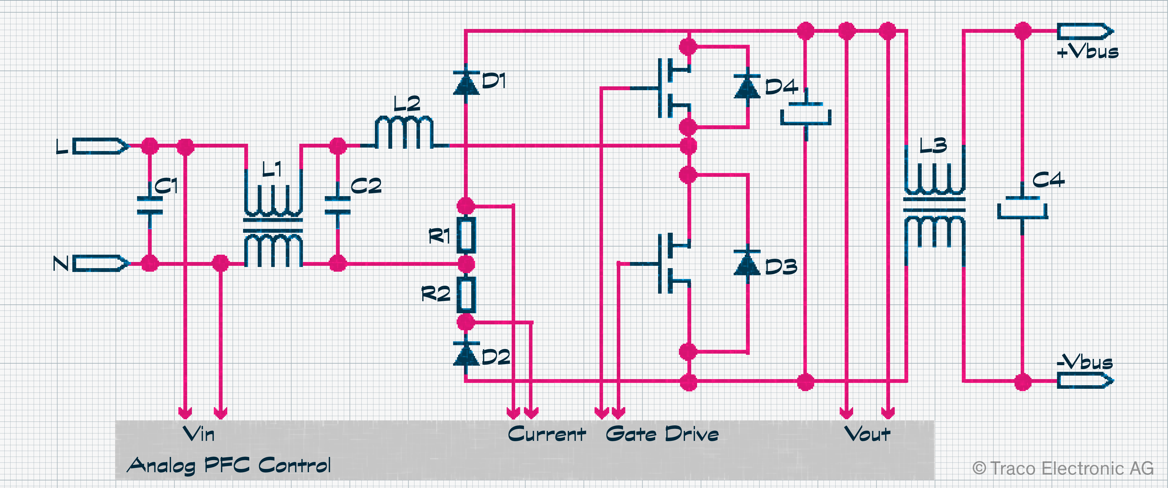
To explore the advantages of GaN in the PFC stage, Traco Power undertook a design study based upon a Totem Pole approach for a power of 1,000 W and 110 VAC to 230 VAC input. The goal was to explore how the switching losses could be reduced when moving away from a silicon-based design to 80 mΩ GaN transistors. Removing the four-diode mains rectifier was one step, as this contributes relatively high forward losses, replacing it with a two-diode implementation (Figure 2).
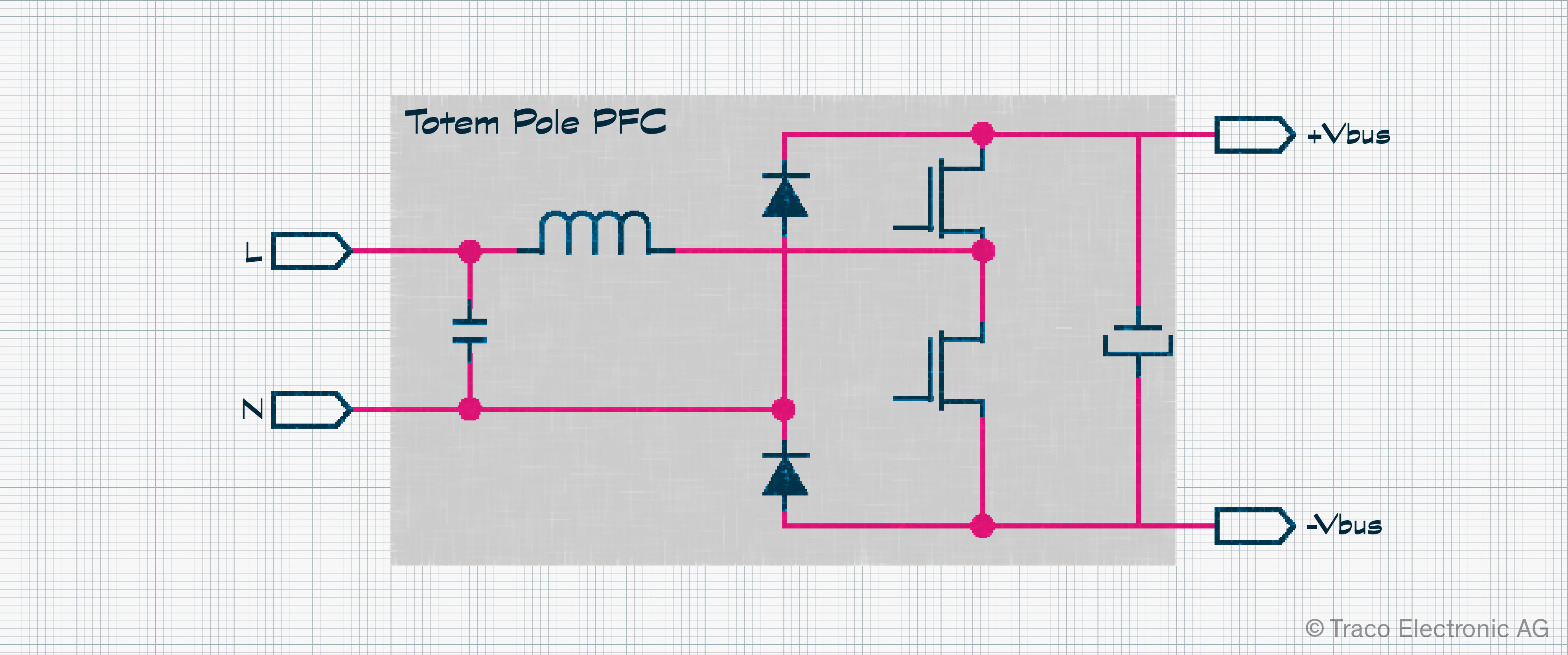
Thanks to the low switching losses of the GaN transistors, the PFC can be operated with a continuous inductor current. With the current in the rectifier diodes and inductor well controlled, the diodes may also be replaced by super junction MOSFETs that, thanks to their low on-resistance, further reduce losses and increase efficiency.
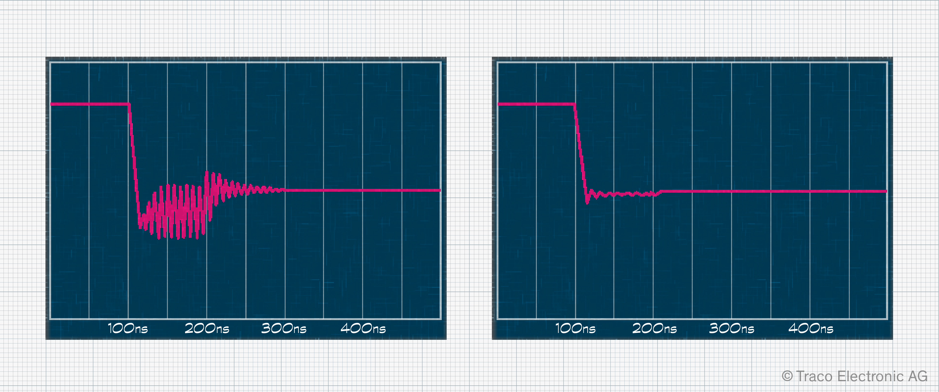
With a switching time of just a few nanoseconds, parasitic inductances and capacitances around the GaN devices lead to very high frequency oscillations at the input and output (Figure 3). Thus, the layout of the PCB requires even more care than usual. To combat this, filters were added at the input. SiC diodes were also added in parallel to the GaN transistors to combat the oscillations occurring when the devices were in reverse conduction (gate off).
This experimental PFC was switched at around 100 kHz, enabling use of smaller inductors using materials with a high magnetic flux density, despite the relatively high re-magnetization losses. There remains room to increase the switching frequency further, supporting higher power densities. As is to be expected, the largest ripple currents occur at the largest difference between input and output voltage. Therefore, heat dissipation should be dimensioned for this most unfavorable operating case.
Challenges relating to GaN use in PFCs
By far the most significant challenge results from the square-wave currents and voltages caused by the very short switching times supported by GaN. The steep on/off edges and high-frequency signals coursing around the circuit demand suitable filtering to fulfill electromagnetic interference (EMI) requirements. Common mode noise is another challenge resulting from parasitic capacitances to ground.
Benefits of GaN in PFCs
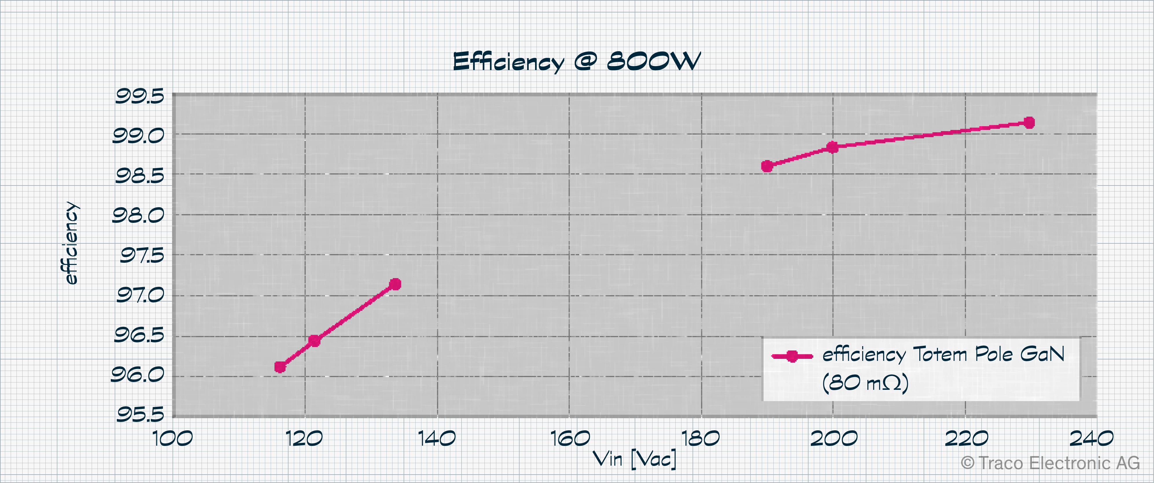
Thanks to the ability to switch in under seven nanoseconds, around ten times faster than conventional MOSFETs, measured turn-on/off losses drop by a similar amount when using GaN transistors. This enables the construction of a PFC that is between 3% and 5% more efficient than a conventional design using silicon MOSFETs and a four-diode rectifier. At high input voltages (230 VAC), efficiencies of over 99% can be achieved (Figure 5). When coupled with a resonant converter, a complete power supply can attain an efficiency of 96%. However, economic challenges hinder selecting GaN for designs targeting lower input voltages or power delivery under 1,000 W.
GaN transistors clearly open a path to higher efficiencies, higher power densities, and smaller form factors. In turn, this enables those using power suppliers, such as designers of servers, to innovate in the products they develop. As power supply designers become more acquainted with their capabilities, component price falls, and the inevitable higher levels of integration take place, it’s clear that GaN is set to take on a significant role in the world of power conversion.