EMC Phenomena – Part 1
Testing for and Protecting Against Electromagnetic Phenomena – Part 1
When developing a new product, the main focus is on its functionality. But something that can bring the entire project screeching to a halt just before production starts is electromagnetic compatibility (EMC) testing. As covered in our blogs on the topic (How to tackle electromagnetic compatibility (EMC) – Part 1 and Part 2), EMC encompasses four key aspects: emissions, immunity, signal integrity, and electrostatic discharge (ESD). In this first of several blogs on this topic, we look closely at some phenomena encompassed by electromagnetic susceptibility (EMS) and electromagnetic interference (EMI). We’ll link them to their associated standards, provide testing tips, and offer methods for resolving testing failures.
Electromagnetic Susceptibility (EMS)
Electrostatic Discharge
We’ve all experienced the “click” of an ESD zap as we’ve climbed out of a car or gone to shake hands with a friend or colleague. The voltage can range from around 8 kV to well beyond 15 kV. And while we often think the zap is the result of touching something, the voltages involved can be so high that the discharge actually occurs through the air. So even though your electrical application may not have metal parts that are exposed enough to be touched, such as a data connector, merely coming close with a hand could be enough for a discharge to occur.
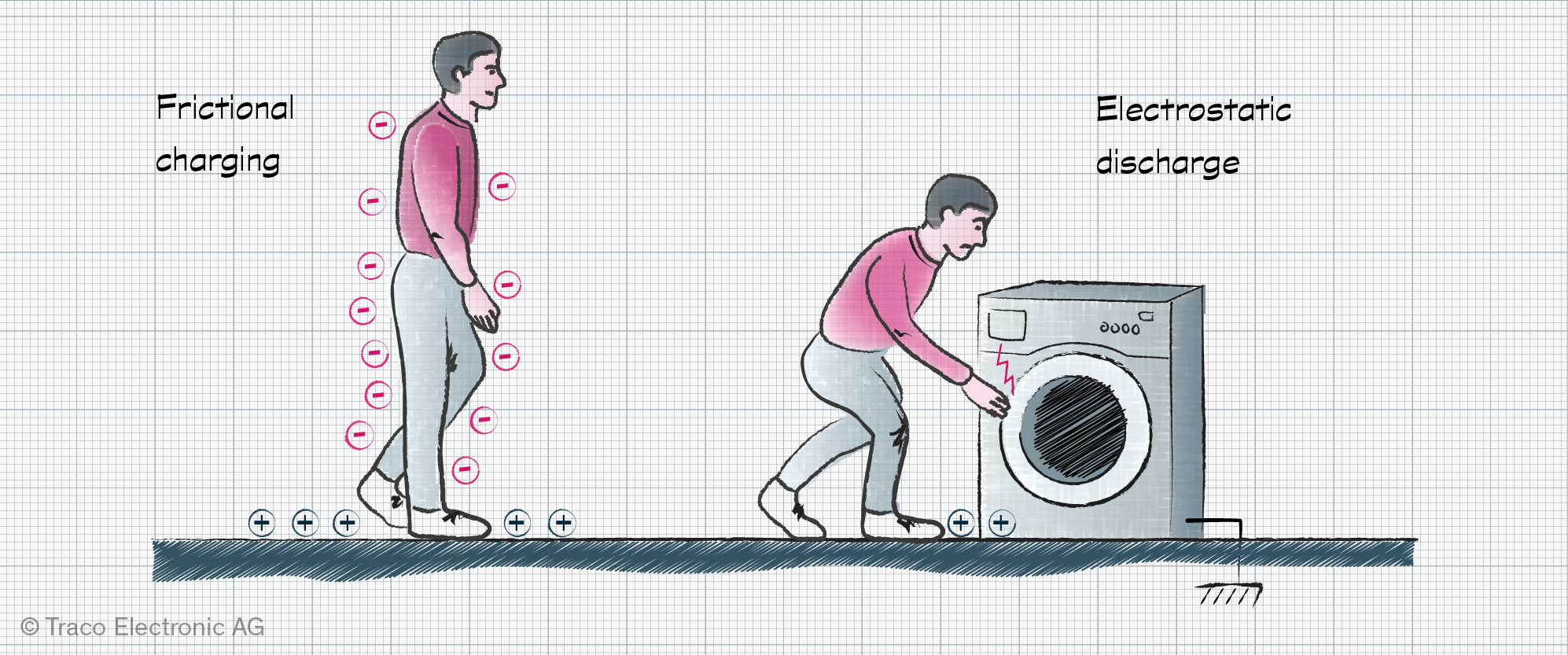
The data lines of such a connector or the terminals of a power supply lead back to an integrated circuit, so the ESD pulse could discharge to ground through that semiconductor device. This can lead to silicon or metallization structures melting or a hole being punched in the oxide. A failure may result immediately. However, a worse outcome is that the resultant weakness slowly leads to failure. In the meantime, the results of this ESD damage may be experienced as intermittent failures in functionality.
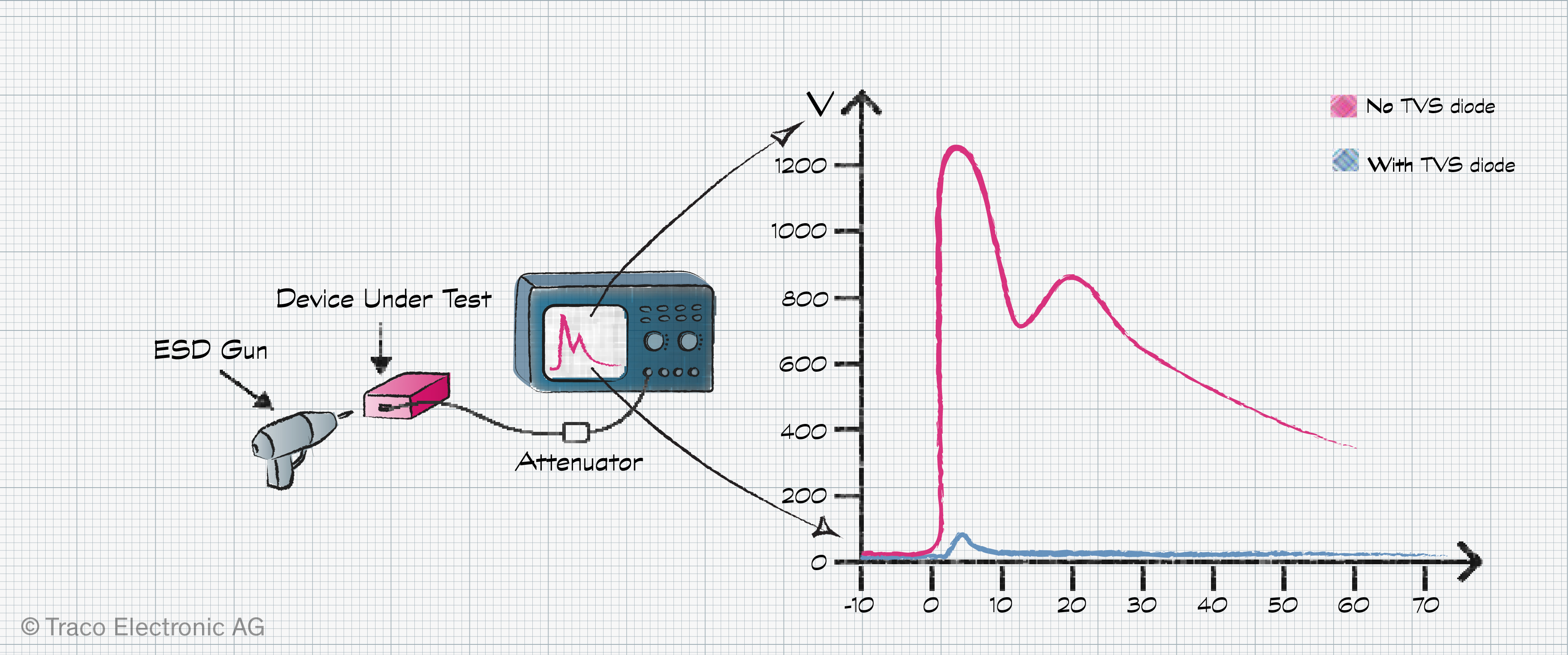
Testing is performed using an ESD gun that, ideally, is placed in contact with an exposed conductive surface. If none is available, air discharge can be used. However, the results are highly dependent on factors such as humidity and even the angle of the ESD gun and its tip shape. It should be noted that such testing is considered destructive, as tests are repeated with increasing voltage until the system’s limit is found.
Susceptible signals can be protected, and a transient voltage suppressor (TVS) diode is often used. Placed between the signal and ground, the TVS diode has little discernable impact on the signal under normal conditions. However, the voltage is discharged through the diode to ground upon application of an ESD pulse. The component’s datasheet typically provides ESD waveforms, and you can expect the peak voltage to be limited to tens of volts for a few nanoseconds.
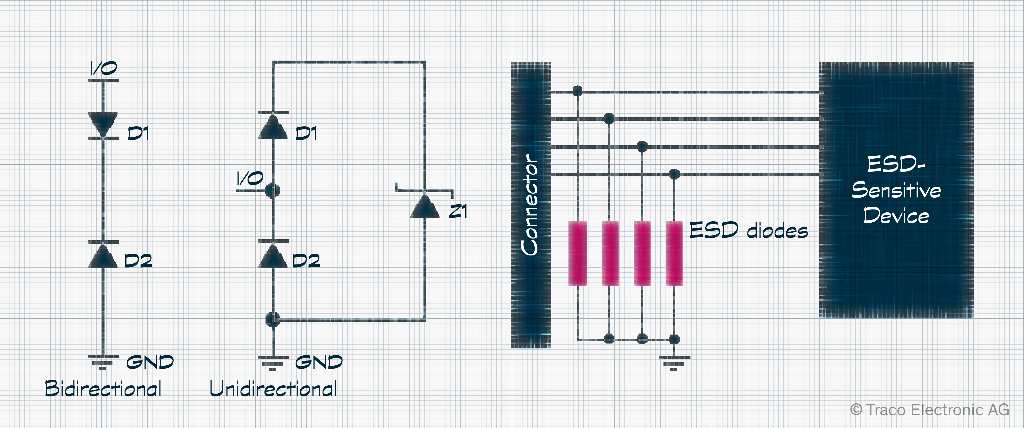
The choice of TVS depends on several factors. The standoff voltage must be higher than your application’s maximum operating voltage. If not, the signal will be clamped under regular operation. You’ll also need to consider whether unidirectional (signal consistently above/below the reference voltage, typically ground) or bidirectional protection is required. High-speed signals, such as USB, demand bidirectional TVS devices with a low capacitance to minimize their impact on signal integrity.
It’s also possible to measure the effect of an ESD discharge. The EN 61000-4-2 standard provides diagrams that describe a suitable setup and the required test equipment. An oscilloscope with a bandwidth of 2 GHz is needed, although some standards demand 16 GHz or more. A sampling rate of 20 giga sample per second displaying at 20 ns/div is sufficient to acquire and check the ESD pulse shape. To avoid damage to the input, attenuators should be placed in the signal path. Some advanced oscilloscopes even provide preset configurations suitable for ESD testing.
Finally, don’t forget to ensure your laboratory is equipped with suitable ESD equipment when handling electronic devices and systems. This can include mats, shoes, wrist straps, containers, and an ESD test station.
Electromagnetic Radiated Field
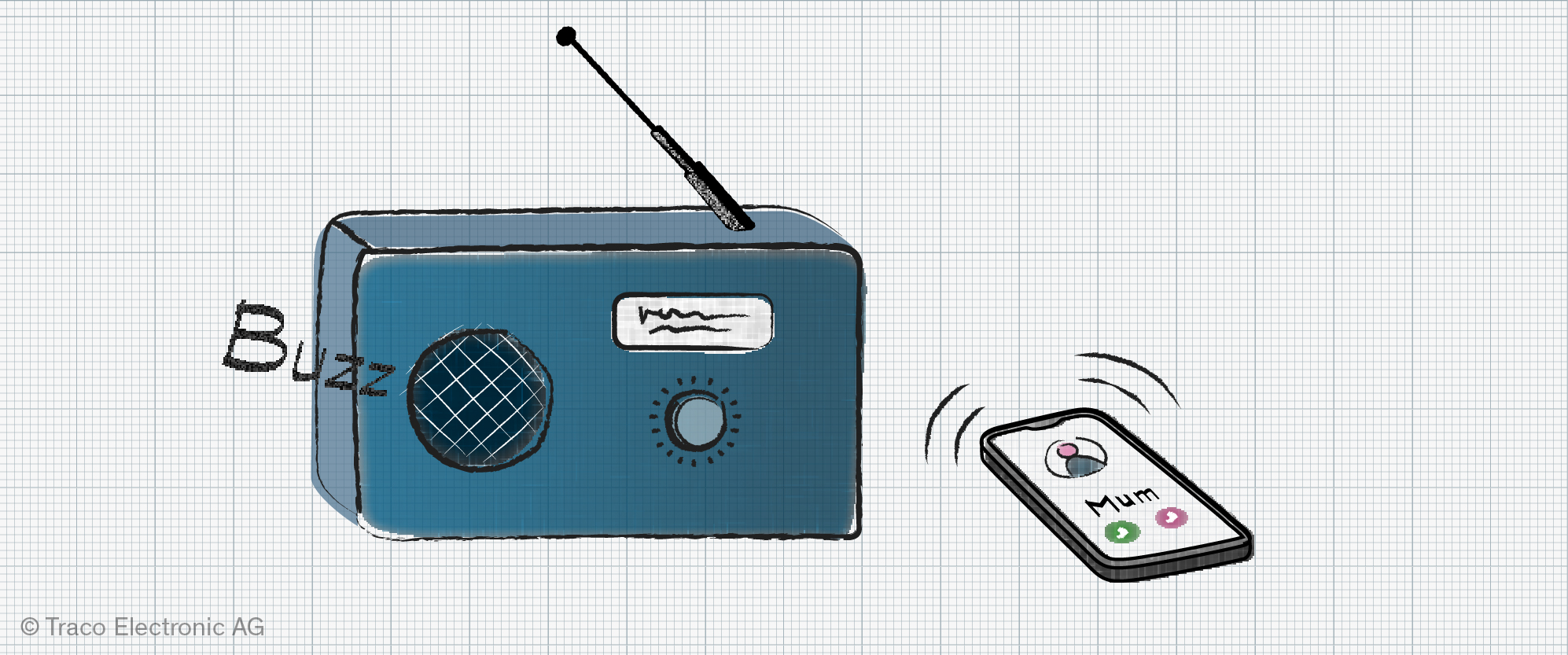
You may have noticed an annoying hum from your car radio when driving past some buildings or heard a buzzing noise shortly before your smartphone rings with a call. If so, you’ve experienced the impact of an electromagnetic radiated field on an electronic system. Typically, this is nothing more than annoying, especially if you were trying to catch the news or traffic report. But in other situations, it could be life-threatening. Pacemakers, medical equipment, or industrial systems that are safety critical may stop working and could cause injury or loss of life in such cases.
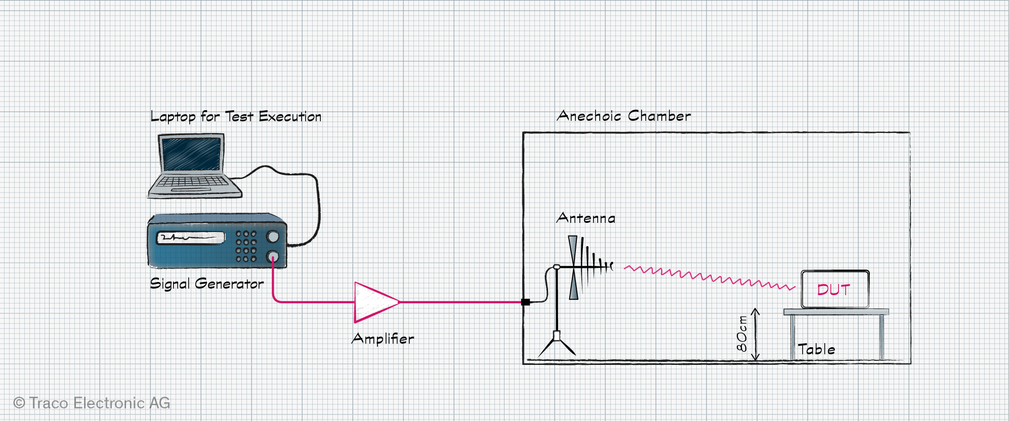
EN 61000-4-3 defines the immunity requirements and testing procedure for radiated continuous radio-frequency. Testing uses a signal generator connected via an amplifier to an antenna pointed at the device under test (DUT). The DUT is then monitored for any abnormalities in operation as a sine-wave-modulated signal is swept across the frequency ranges 80 MHz to 1 GHz, or 800 MHz to 960 MHz and 1.4 GHz to 6 GHz. The field strength applied depends on the environment the application will be exposed to in normal operation. Additionally, your product must be tested with any cables and accessories required for operation.
Because of the risk of interfering with other equipment, such tests are executed inside an anechoic chamber. Thus, you’re unlikely to be able to perform these tests in your own laboratory.
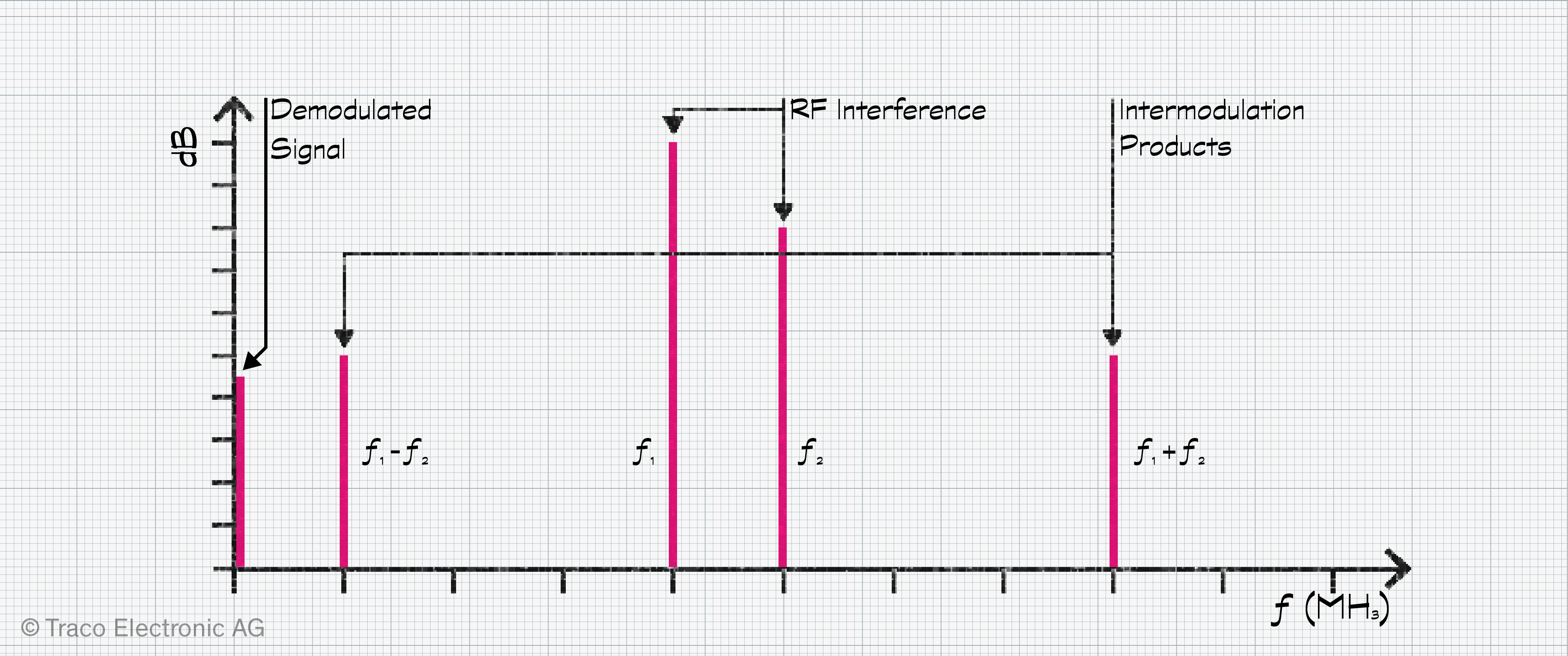
While the standard provides a uniform testing process, it won’t necessarily find any issues with your application. One weakness is the use of a single modulated frequency. In the real world, devices are subjected to many frequencies simultaneously. These can produce intermodulation products, signals that may influence your application’s measurements. Furthermore, silicon devices demodulate radio signals, often resulting in interference at the low sampling frequencies used for data acquisition and impacting measurement accuracy.
The frequency range used for testing is quite high, but your circuit may be more susceptible to signals below 80 MHz. In this case, potential issues may only come to light when testing against EN 61000-4-16 (immunity to conducted noise) that focuses on the 0 Hz to 150 kHz range.
Another practical difficulty is placing the DUT in all relevant operational modes during testing and monitoring the result. Typically, the tests are executed unattended, requiring some sort of remote viewing and control of the device. It may be necessary to execute some custom software during testing, and a dwell time may be required during sweeps to provide time to see any negative response to the applied signal.
In the event of a failure, the team will learn at which frequencies their device is susceptible. To replicate the issue in your lab, localized signal generation at the frequencies of interest could be attempted, or you could undertake testing in a portable shielded tent before reattempting any certification. This can be done with near-field probes, RF injection, or even a radio transmitter in the ISM band.
There are three ways to tackle interference issues: filtering, grounding, and shielding. You’ll need to determine the problematic part of the circuit, how the issue manifests itself, and which remedy works best. If your application uses software configurable parts, changes to filter setup or clock frequencies may also be part of the solution. However, once you resolve the issue at the frequency of interest, you also need to be sure that the issue hasn’t unintentionally been pushed to another.
While formal testing proves that EN 61000-4-3 can be fulfilled, most system designers understand the specific radiated field challenges where their application is typically used. For example, touchscreen designers understand that noise from home appliances can impact operation. If you know your application will be used near equipment that has previously caused issues, it is worth testing it in situ as part of your test regime.
Stay Methodical when Fixing Issues
Regardless of ESD or EMI, working methodically through tests and changes is essential to their resolution. Only make one change at a time, where possible, and record your results. Photos of your setup also help replicate the test environment at a later date. If you’re working with an antenna and the DUT, make sure to mark the position of all equipment with some tape. Finally, don’t forget to lift and move cables, switch off other local equipment, and locate the position of any transmitters in your area to discount other sources of interference.
If you want to read more about EMC Phenomena, please continue to the second part or third part of the three-part series.
Return to the Traco Power Corner again soon to learn about other electromagnetic phenomena, such as electrical fast transients, surges, and conducted radio frequency field testing.